Thanks to recent research and development efforts, the electronics industry is rapidly moving towards flexible and lightweight devices, realized through a variety of possible designs. For example, one popular approach is the manufacture of electronic devices on deformable polymer substrates, where a thin layer of conducting material overlies the polymer. Over the last five years, this has been a research focus of Dr Megan Cordill from the Erich Schmid Institute for Materials Science and the University of Leoben (Austria), and her group is looking specifically at the mechanical behavior of brittle and ductile materials under strain.
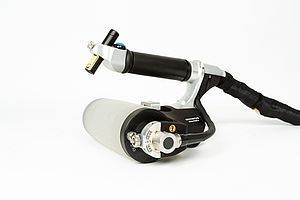
How the microstructure of ductile films affects their electrical and mechanical behavior during mechanical loading reflects the strength and electrical resistance of the film, as well as its adhesion to the substrate. For these investigations, a mechanical straining stage device is controlled automatically for loading or unloading at a certain rate, and through coupling the device to a high-resolution imaging system, sample displacement and electrical resistance can be measured in parallel. Termed the ‘in situ squared’ method by Dr Cordill’s group, cycles of strain replicate the fatigue the device would suffer outside of the laboratory.
The in situ squared system
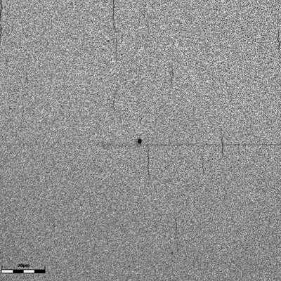
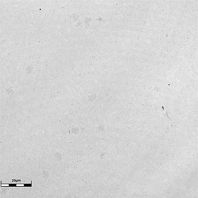
In situ electromechanical testing yields many advantages, not least overcoming the complications owing to the viscoelastic recovery of the polymer after the sample is unloaded. Interestingly, as the polymer substrate relaxes to compress the overlying film, observing the sample after unloading can mask any cracks and the sample may appear unaffected. Moreover, the sample will have a much lower electrical resistance than it did at the maximum loading, and it is important to consider this alongside the maximum resistance. Holding the sample for longer reveals any cracks, and therefore in situ testing is vital for visualizing deformation or fracture (Figure 1).
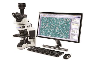
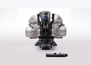
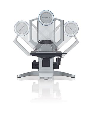
While Dr Cordill’s work has relied heavily on the high resolution afforded by atomic force microscopy (AFM) observation, the introduction of confocal laser scanning microscopy (CLSM) with the Olympus LEXT OLS4100 has now opened many doors for analysis. Using CLSM, the experiment can be stopped at certain levels of strain, including a hold period of three minutes before acquiring the images, and this has proved beneficial in a range of studies. With the ability to measure delamination alongside electrical and mechanical properties in situ, the LEXT OLS4100 provides a comprehensive picture of thin film behavior under loading conditions.
Observing behavior: AFM or CLSM?
The depth of insights offered by in situ squared testing are highly dependent on the observation technique employed. Dr Cordill’s group have found both CLSM and AFM provide information linking crack evolution as a function of strain, with the following comparisons:
• Field of view: Only a small area (~20-25 µm) could be visualized by AFM compared to CLSM, limiting observations to 4-5 cracks per image and failing to provide meaningful statistics.
• Accessibility: Acquiring high quality images with AFM requires experience, and repeat inspection of the same area is challenging. Instead, CLSM is straightforward, designed to enable every user to acquire high-quality images.
• Speed: AFM is slower, with one experiment taking up to one day.
Layers – less is more
With the research of Dr Cordill’s group, it is becoming increasingly clear that in certain film systems with certain microstructures, adhesion layers can prove detrimental to electromechanical behavior. In the rigid electronic industry it was historically thought that gold and copper have low adhesion to polymers, and so additional layers were introduced. Although this was not the case according to the literature of the 1980’s, it was assumed that the interlayer would still be needed in the flexible electronic industry. Dr Cordill’s work is instead showing that these interlayers are actually damaging. For example, when a chromium layer sits between a copper and polymer layer, the chromium film has very low fracture strain and cracks form in this layer first. These cracks subsequently act as stress concentration points and cause cracks to form in the overlying copper layer – forming much faster than a film with just a copper layer (Figure 2). Without the chromium adhesion layer, after 100 cycles cracks are only just beginning to form.1
Summary
Flexible electronic devices must withstand bending, stretching and twisting, and linking electrical and mechanical properties under strain provides unprecedented insights into the behavior of thin film devices. The innovative work of Dr Cordill’s group has reinvented the design of flexible electronic devices, demonstrating how the inclusion of an adhesion layer is detrimental and leads to cracking in the case of copper. Shedding light on the behavior of these devices in more detail than ever before was made possible through looking beyond AFM, coupling in situ testing with the fast and easy-to-use Olympus LEXT OLS4100. This technology provides a fast means to generating new information, allowing manufacturers to determine when cracks form, guiding the optimization process and leading us towards robust, market-ready devices.


