Analog Devices. The LTC3372 is a highly integrated dc-to-dc converter solution suited for automotive, telecommunication, industrial, and other applications that require multiple low voltage rails derived from input voltages up to 60 V. The LTC3372 contains both high voltage and low voltage converter systems within its thermally enhanced 48-lead, 7 mm × 7 mm package. The high voltage (HV) buck controller can step down an input voltage of up to 60 V to a pin-programmed 5 V or 3.3 V. This 5 V or 3.3 V output is then used to feed the LTC3372’s configurable, multiple output, multiphase low voltage (LV) monolithic buck regulator.
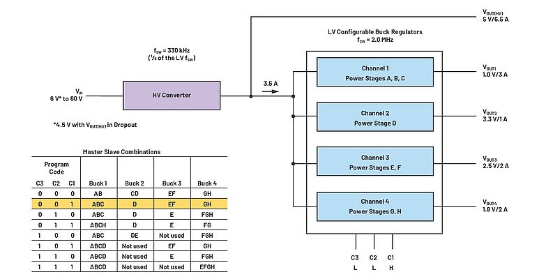
This low voltage portion of the LTC3372 consists of eight 1 A, parallelable power stages. These stages can be arranged in a number of ways to provide two, three, or four channels, with each channel consisting of one to four stages each, depending on the per channel load requirements. As shown in Figure 1, up to eight different configurations are possible by setting the bits at C3, C2, and C1. This level of flexibility allows the designer to use one IC for a wide variety of designs with a minimal number of external components and a small overall footprint. In addition, the output of each channel can be set from 0.8 V to LVIN. The switching frequency range is 1 MHz to 3 MHz.
The HV controller drives external N-channel MOSFETs and operates over a 4.5 V to 60 V input voltage range. Depending on the component selection and layout, the HV converter can support load currents over 20 A. This is enough to satisfy the demands of the LV regulators in addition to the system loads riding on the HV output. With only the HV controller on and providing 5 V, the no load Burst Mode® IQ is 15 μA, yielding high efficiency at light loads. An internal clock divider sets the switching frequency of the HV converter to 1/6 of the LV frequency.
45 W, 5-Output, Compact Converter from a 6 V to 60 V Input
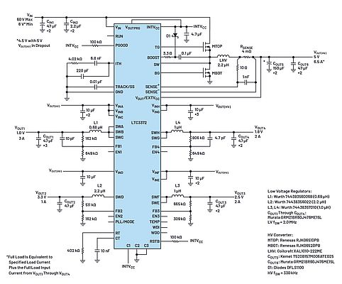
Figure 1 and Figure 2 show the block diagram and schematic of an LTC3372-based solution, respectively. Its LV regulator section provides outputs of 1.0 V at 3 A, 3.3 V at 1 A, 1.8 V at 2 A, and 2.5 V at 2 A, at a switching frequency of 2 MHz from the 5 V output of the HV converter (labeled as VOUT(HV)). The 5 V HV rail supplies 6.5 A to the system and 3.5 A to the input of the LV regulators at a switching frequency of 330 kHz. The input voltage range of the HV converter is 6 V to 60 V. This converter can be powered from a wide variety of sources, including a 12 V automotive battery with surges up to 60 V, a 48 V telecom or automotive battery, or an offline supply. The high level of integration and the 2 MHz switching frequency of the LV regulators allow the solution to fit a 2.2 in2 footprint.
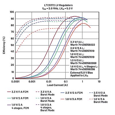
As shown in Figure 1 and Figure 2, the LV regulators are set up for the ABC-D-EF-GH configuration by setting pins C3 and C2 low and pin C1 high and tying the appropriate SW nodes together. By paralleling enough 1 A power stages to satisfy the maximum load requirement—and not more—the efficiency peaks around 50% load, where the typical sustained loads occur. Adding more stages results in higher full load efficiency, but lower efficiency at mid loads. If, for instance, the 1.8 V/2 A LV rail was built from four paralleled power stages instead of two, the efficiency would be lower for loads of 50% or less in FCM—see Figure 3. When Burst Mode operation is selected, the efficiency stays high over a broad range of loads. The efficiency of the 1.8 V/2 A rail is 82.2% and higher for load currents of 1 mA and above.
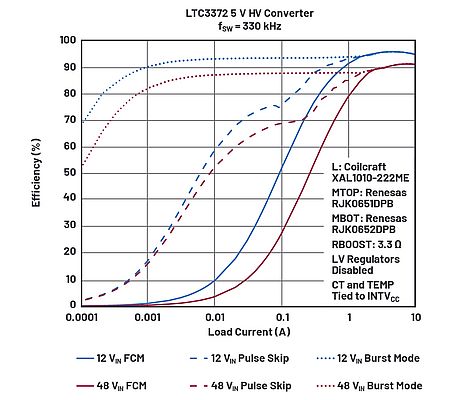
The strong gate drivers of the LTC3372 HV provide the HV 5 V rail with a full load efficiency of 94.6% at 12 V input and 90.9% at 48 V input—see Figure 4. With Burst Mode operation selected, the efficiency is 90.1% for a load of 1 mA and a 12 V input.
High Level of Integration in a Small Package
The LTC3372 comes in a thermally enhanced 48-lead, 7 mm × 7 mm package. Additional features of the LTC3372 include: a PLL/MODE pin to either synchronize the controller to an external clock or program light load operating modes of forced continuous mode, Burst Mode operation, or discontinuous mode (HV only); a watchdog input and output; a TEMP pin to monitor die temperature; a PGOOD pin for the HV converter; an RSTB pin for the LV regulators; and more.
Conclusion
The LTC3372 provides the designer with a flexible, highly integrated solution for providing multiple outputs from a high input voltage. Its HV converter can provide a 5 V or 3.3 V output from input voltages up to 60 V. From this intermediate rail, the monolithic LV regulator can provide up to four outputs with maximum output currents ranging from 1 A to 4 A and voltages down to 0.8 V.
Michael Shriver, Senior Applications Engineer - Analog Devices


